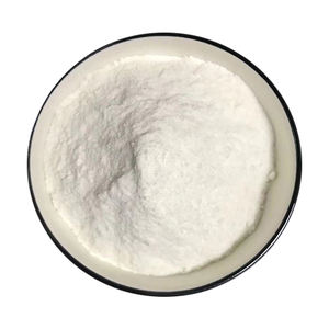
Overview of Semiconducting Material Selenide Antimony Sb2Se3 CAS No.1315-05-5
Telluride and selenide compounds play a significant role in the field of semiconductors, particularly in the development of advanced electronic and optoelectronic devices. These materials belong to the chalcogenide family, characterized by their ability to form compounds with elements from groups IV-VI in the periodic table.
Tellurides: Compounds containing tellurium (Te) as the chalcogen. Examples include cadmium telluride (CdTe), mercury telluride (HgTe), and zinc telluride (ZnTe). These materials have found applications in solar cells, infrared detectors, and high-speed electronics due to their tunable bandgap, high electron mobility, and good thermal stability.
Selenides: Similar to tellurides, but with selenium (Se) replacing tellurium. Notable examples are cadmium selenide (CdSe), gallium selenide (GaSe), and zinc selenide (ZnSe). Selenide compounds are widely used in light-emitting diodes (LEDs), laser diodes, and solar cells due to their direct bandgap properties and efficient light absorption/emission capabilities.
Feature of Semiconducting Material Selenide Antimony Sb2Se3 CAS No.1315-05-5
Direct Bandgap: Many telluride and selenide semiconductors have direct bandgaps, which facilitate efficient light emission and absorption processes. This makes them suitable for optoelectronic applications such as LEDs and lasers.
Tunable Bandgap: The bandgap of these materials can be adjusted by alloying or altering the composition (e.g., CdSe to CdTe), enabling customization for specific device requirements across a wide spectrum of wavelengths.
High Electron Mobility: Materials like HgCdTe exhibit high electron mobility, which is crucial for high-speed electronic devices and low-noise detector applications.
Thermal Stability: Some tellurides and selenides, like ZnTe and ZnSe, demonstrate good thermal stability, making them suitable for high-temperature operation and processing.
Non-Toxic Alternatives: With increasing environmental concerns, there’s a push towards exploring less toxic alternatives to commonly used semiconductors. For instance, Cd-based tellurides and selenides are being replaced or combined with less toxic elements like Mg or Mn in some applications.
(Semiconducting Material Selenide Antimony Sb2Se3 CAS No.1315-05-5)
Parameters of Semiconducting Material Selenide Antimony Sb2Se3 CAS No.1315-05-5
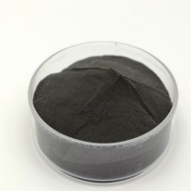
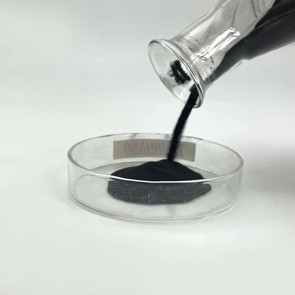
Selenide antimony, also known as Sb2Se3, is a fascinating and technologically significant semiconducting material with the Chemical Abstracts Service (CAS) number 1315-05-5. This inorganic compound belongs to the group of chalcogenides, where selenium (Se) and antimony (Sb) atoms form a unique crystal lattice structure. The chemical formula Sb2Se3 suggests that there are two atoms of antimony for every three atoms of selenium, creating a stoichiometry that makes it an interesting material for various applications.
The compound’s crystalline structure is primarily rhombohedral, which means it has a non-cubic arrangement of atoms. Its lattice parameters give it a distinct physical appearance and properties. Sb2Se3 exhibits a layered structure, with alternating layers of Sb and Se atoms, allowing for both high thermal stability and flexibility, making it suitable for thin-film applications.
As a semiconductor, Sb2Se3 falls into the intermediate bandgap category, with an energy gap between its valence and conduction bands. This feature enables it to be neither a conductor nor an insulator, but rather, a p-type semiconductor, meaning it can easily accept holes (positive charge carriers) when doped with certain elements. The bandgap lies around 1.8 eV, which is relatively low compared to other semiconductors like silicon or gallium arsenide, making it more sensitive to light and suitable for optoelectronic devices.
One of the most notable properties of Sb2Se3 is its ability to change its electronic properties through phase transitions. Under specific temperatures, it undergoes a topological transition from a trivial insulator to a topological insulator, where the bulk is insulating while the surface states are metallic. This property, known as topological protection, makes it a promising candidate for applications in quantum computing and spintronics.
Moreover, Sb2Se3 has shown potential in thermoelectric applications due to its relatively high Seebeck coefficient, a measure of the voltage generated per temperature difference across a material. This material’s combination of high electrical conductivity and low thermal conductivity makes it an attractive choice for waste heat recovery and thermoelectric generators.
In recent years, research on Sb2Se3 has expanded to include its use in nanotechnology and nanomaterials. It has been synthesized in various nanostructures such as nanowires, quantum dots, and thin films, which can enhance its performance in devices like solar cells, sensors, and transistors. Additionally, its compatibility with other materials like graphene and metal oxides opens up possibilities for hybrid systems with improved functionalities.
However, challenges remain in scaling up production and optimizing its properties for commercial use. The synthesis process often involves complex methods, and environmental concerns related to the use of antimony need to be addressed. Nevertheless, the unique properties of Sb2Se3 make it a promising material with a promising future in the realm of electronics, energy conversion, and advanced materials science.
In conclusion, Sb2Se3, with its CAS number 1315-05-5, is a versatile and intriguing semiconducting material. Its layered structure, tunable electronic properties, and topological characteristics make it an essential component in the development of innovative technologies. As researchers continue to explore its potential, Sb2Se3 holds the promise to contribute significantly to the evolution of modern electronics and energy-related industries.
(Semiconducting Material Selenide Antimony Sb2Se3 CAS No.1315-05-5)
FAQ of Semiconductor Materials
Inquiry us
