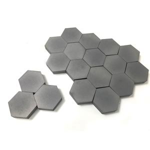

Overview of P type N type bismuth telluride Bi2Te3
Telluride and selenide compounds play a significant role in the field of semiconductors, particularly in the development of advanced electronic and optoelectronic devices. These materials belong to the chalcogenide family, characterized by their ability to form compounds with elements from groups IV-VI in the periodic table.
Tellurides: Compounds containing tellurium (Te) as the chalcogen. Examples include cadmium telluride (CdTe), mercury telluride (HgTe), and zinc telluride (ZnTe). These materials have found applications in solar cells, infrared detectors, and high-speed electronics due to their tunable bandgap, high electron mobility, and good thermal stability.
Selenides: Similar to tellurides, but with selenium (Se) replacing tellurium. Notable examples are cadmium selenide (CdSe), gallium selenide (GaSe), and zinc selenide (ZnSe). Selenide compounds are widely used in light-emitting diodes (LEDs), laser diodes, and solar cells due to their direct bandgap properties and efficient light absorption/emission capabilities.
Feature of P type N type bismuth telluride Bi2Te3
Direct Bandgap: Many telluride and selenide semiconductors have direct bandgaps, which facilitate efficient light emission and absorption processes. This makes them suitable for optoelectronic applications such as LEDs and lasers.
Tunable Bandgap: The bandgap of these materials can be adjusted by alloying or altering the composition (e.g., CdSe to CdTe), enabling customization for specific device requirements across a wide spectrum of wavelengths.
High Electron Mobility: Materials like HgCdTe exhibit high electron mobility, which is crucial for high-speed electronic devices and low-noise detector applications.
Thermal Stability: Some tellurides and selenides, like ZnTe and ZnSe, demonstrate good thermal stability, making them suitable for high-temperature operation and processing.
Non-Toxic Alternatives: With increasing environmental concerns, there’s a push towards exploring less toxic alternatives to commonly used semiconductors. For instance, Cd-based tellurides and selenides are being replaced or combined with less toxic elements like Mg or Mn in some applications.
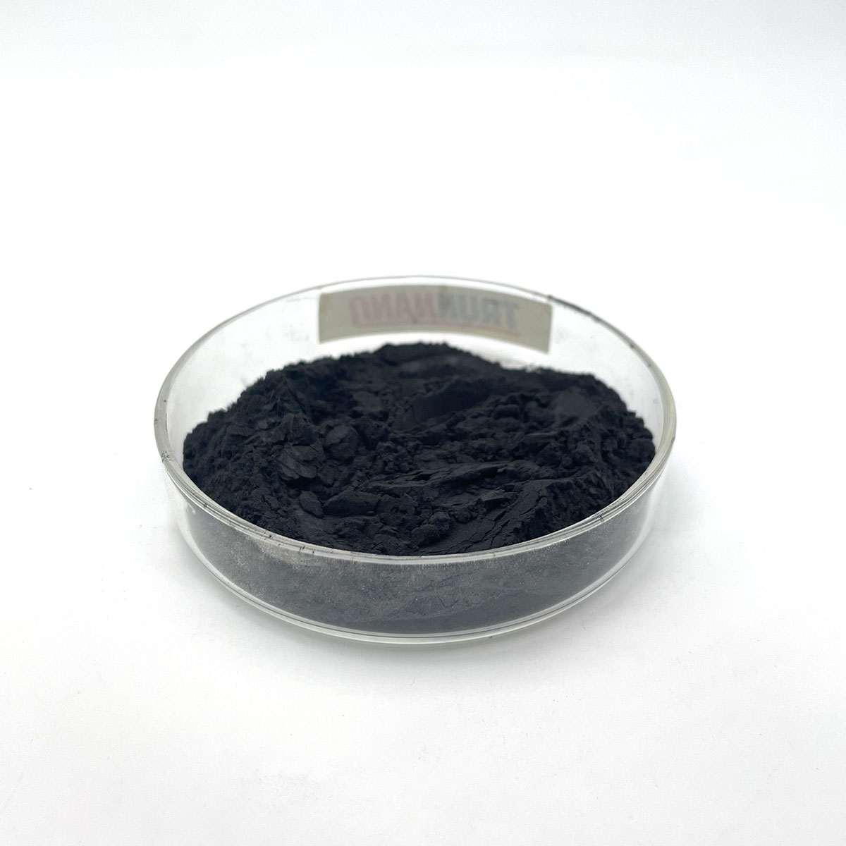
(P type N type bismuth telluride Bi2Te3)
Parameters of P type N type bismuth telluride Bi2Te3
Bismuth Telluride (Bi2Te3), a fascinating material in the realm of condensed matter physics, is a ternary chalcogenide semiconductor that has garnered significant attention due to its unique properties and potential applications in various fields, including thermoelectrics, optoelectronics, and spintronics. As a p-type and n-type doped compound, it exhibits intriguing electronic behavior.
The chemical formula Bi2Te3 represents a combination of two elements, bismuth (Bi) and tellurium (Te), forming a crystal structure typically described as rhombohedral or hexagonal, with a space group R-3m. The compound consists of layers of Te atoms sandwiched between layers of Bi atoms, creating a stacking sequence that influences its electronic band structure.
In its intrinsic form, Bi2Te3 is an indirect bandgap semiconductor, with an energy gap around 0.15 to 0.2 eV at room temperature. This small bandgap allows for relatively efficient charge carrier transport, which is crucial for thermoelectric applications where converting temperature differences into electrical power. The p-type doping introduces holes (positive charge carriers) by introducing impurities like copper (Cu), silver (Ag), or gold (Au), which donate electrons to the valence band, lowering the Fermi level and increasing the hole concentration.
On the other hand, n-type doping is achieved by introducing electron donors like antimony (Sb), selenium (Se), or arsenic (As). These dopants replace Te atoms, creating localized states within the conduction band, which facilitates the movement of free electrons. The n-type doping increases the electron concentration, making it possible to control the carrier balance in the material.
One of the key parameters in Bi2Te3 is its Seebeck coefficient, which measures the voltage generated per unit temperature difference across the material. Its high value, typically around 700 to 800 μV/K, makes it an attractive candidate for thermoelectric devices. Additionally, Bi2Te3 has a high electrical conductivity, particularly when doped, which enhances its thermoelectric figure of merit (ZT), a dimensionless metric that quantifies the efficiency of a thermoelectric material.
Another parameter worth mentioning is the thermal conductivity, which can be manipulated through nanostructuring or alloying to improve the thermoelectric performance. By reducing phonon scattering, one can enhance the ZT value, making Bi2Te3 more competitive in practical applications.
Bi2Te3 also exhibits topological properties, hosting surface states known as the quantum spin Hall effect, which are protected by time-reversal symmetry. This property makes it a promising material for spintronics and topological electronics, where information can be processed using the spin of electrons rather than their charge.
In conclusion, Bismuth Telluride (Bi2Te3) with its p-type and n-type doping capabilities offers a versatile platform for exploring novel electronic phenomena and developing advanced technologies. Its unique combination of band structure, thermoelectric properties, and topological characteristics make it a material of great interest in the scientific community, warranting further research and development.
(P type N type bismuth telluride Bi2Te3)
FAQ of Semiconductor Materials
Inquiry us

