
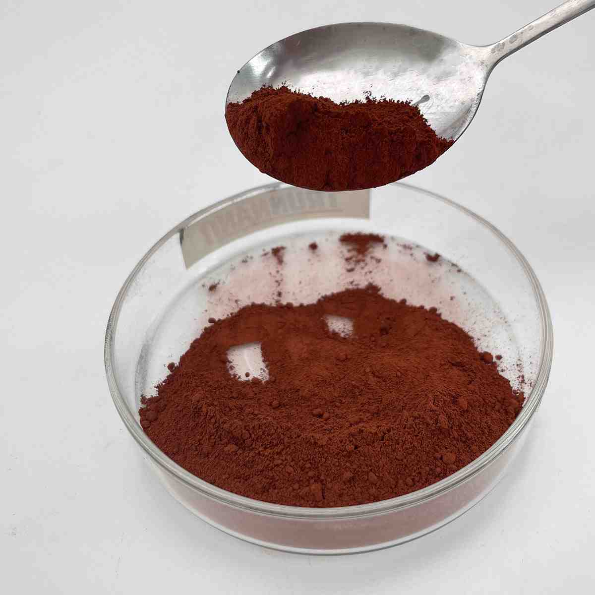
Overview of PVD target Bi2Te3 bismuth telluride sputtering target
Telluride and selenide compounds play a significant role in the field of semiconductors, particularly in the development of advanced electronic and optoelectronic devices. These materials belong to the chalcogenide family, characterized by their ability to form compounds with elements from groups IV-VI in the periodic table.
Tellurides: Compounds containing tellurium (Te) as the chalcogen. Examples include cadmium telluride (CdTe), mercury telluride (HgTe), and zinc telluride (ZnTe). These materials have found applications in solar cells, infrared detectors, and high-speed electronics due to their tunable bandgap, high electron mobility, and good thermal stability.
Selenides: Similar to tellurides, but with selenium (Se) replacing tellurium. Notable examples are cadmium selenide (CdSe), gallium selenide (GaSe), and zinc selenide (ZnSe). Selenide compounds are widely used in light-emitting diodes (LEDs), laser diodes, and solar cells due to their direct bandgap properties and efficient light absorption/emission capabilities.
Feature of PVD target Bi2Te3 bismuth telluride sputtering target
Direct Bandgap: Many telluride and selenide semiconductors have direct bandgaps, which facilitate efficient light emission and absorption processes. This makes them suitable for optoelectronic applications such as LEDs and lasers.
Tunable Bandgap: The bandgap of these materials can be adjusted by alloying or altering the composition (e.g., CdSe to CdTe), enabling customization for specific device requirements across a wide spectrum of wavelengths.
High Electron Mobility: Materials like HgCdTe exhibit high electron mobility, which is crucial for high-speed electronic devices and low-noise detector applications.
Thermal Stability: Some tellurides and selenides, like ZnTe and ZnSe, demonstrate good thermal stability, making them suitable for high-temperature operation and processing.
Non-Toxic Alternatives: With increasing environmental concerns, there’s a push towards exploring less toxic alternatives to commonly used semiconductors. For instance, Cd-based tellurides and selenides are being replaced or combined with less toxic elements like Mg or Mn in some applications.

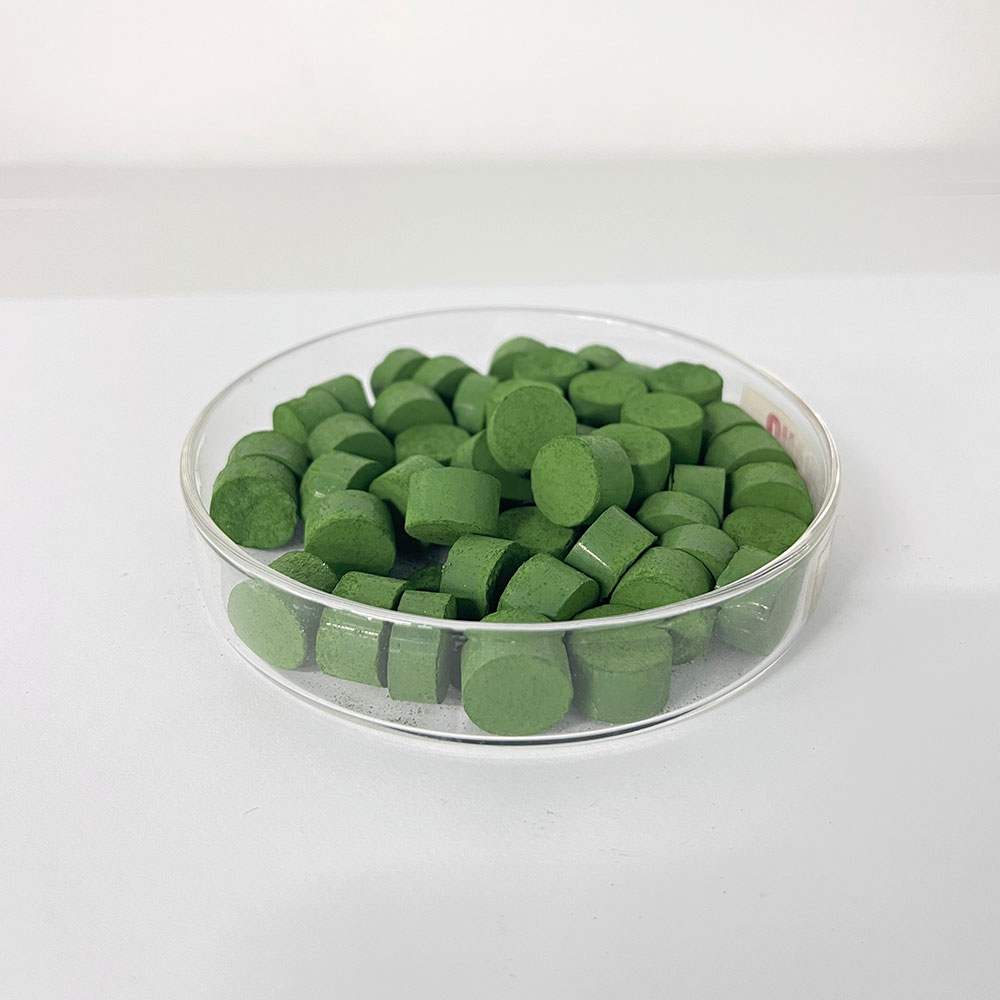
(PVD target Bi2Te3 bismuth telluride sputtering target)
Parameters of PVD target Bi2Te3 bismuth telluride sputtering target
Bismuth Telluride (Bi2Te3), also known as Bi-2Te, is a fascinating material in the field of thin film technology and optoelectronics due to its unique properties, such as high thermoelectric performance, topological insulator behavior, and potential applications in solar cells, thermoelectric generators, and quantum computing. As a PVD (Physical Vapor Deposition) target, Bi2Te3 plays a crucial role in depositing high-quality films for these advanced technologies.
The choice of Bi2Te3 as a PVD target for sputtering is primarily driven by its crystalline structure, which consists of stacked layers of bismuth and tellurium atoms. The material’s tetradymite crystal structure makes it suitable for epitaxial growth, ensuring high-quality films with well-defined orientation and reduced defects. The stoichiometry of Bi2Te3, with a molar ratio of 2:3, ensures that the desired chemical composition is achieved during deposition.
In the context of sputtering, several parameters are essential for optimizing the target’s performance:
1. **Material purity**: High-purity Bi2Te3 targets are crucial, as impurities can lead to detrimental effects on film quality, such as reduced efficiency, increased defects, and variations in electrical and thermal properties. Purity levels above 99.99% are typically required.
2. **Target thickness**: The thickness of the Bi2Te3 target affects the rate of material evaporation during sputtering. Thicker targets provide a more stable source of material, while thinner targets result in faster deposition rates. A balance must be struck between these factors, considering the specific application requirements.
3. **Sputter gas**: The choice of sputter gas, usually argon or a combination of argon and helium, influences the energy transfer from the plasma to the target and the deposited film’s stoichiometry. Argon is commonly used due to its lower cost and compatibility with Bi2Te3.
4. **Sputtering power and pressure**: The power applied to the target and the vacuum chamber pressure determine the deposition rate and film uniformity. Higher powers result in faster deposition but may cause target erosion. Optimal conditions depend on the desired film thickness and the substrate’s thermal budget.
5. **Substrate temperature**: The substrate temperature during deposition affects the film’s growth rate, phase transformation, and adhesion. For optimal thermoelectric performance, the substrate should be heated to a temperature close to the melting point of Bi2Te3 to promote epitaxial growth.
6. **Target geometry**: Different target geometries, such as planar, cylindrical, or diced, can influence the deposition uniformity and target life. Planar targets are popular due to their ease of use and lower cost, but they may require more complex target replacement procedures.
7. **Cooling system**: Effective cooling of the target is necessary to maintain its structural integrity and prevent overheating, which can lead to material degradation and reduced efficiency. Efficient cooling systems minimize temperature gradients across the target surface.
In conclusion, Bi2Te3 as a PVD target for sputtering offers exceptional opportunities in various applications, but achieving optimal deposition conditions requires careful consideration of multiple parameters. By tuning these factors, researchers and engineers can produce high-quality Bi2Te3 films that exhibit exceptional performance and pave the way for next-generation devices.
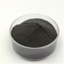
(PVD target Bi2Te3 bismuth telluride sputtering target)
FAQ of Semiconductor Materials
Inquiry us
