Overview of CdSe PVD Materials High Purity MBE Grade 6N (99.9999%) Sputter Target Cadmium Selenide(CdSe) Powder
Telluride and selenide compounds play a significant role in the field of semiconductors, particularly in the development of advanced electronic and optoelectronic devices. These materials belong to the chalcogenide family, characterized by their ability to form compounds with elements from groups IV-VI in the periodic table.
Tellurides: Compounds containing tellurium (Te) as the chalcogen. Examples include cadmium telluride (CdTe), mercury telluride (HgTe), and zinc telluride (ZnTe). These materials have found applications in solar cells, infrared detectors, and high-speed electronics due to their tunable bandgap, high electron mobility, and good thermal stability.
Selenides: Similar to tellurides, but with selenium (Se) replacing tellurium. Notable examples are cadmium selenide (CdSe), gallium selenide (GaSe), and zinc selenide (ZnSe). Selenide compounds are widely used in light-emitting diodes (LEDs), laser diodes, and solar cells due to their direct bandgap properties and efficient light absorption/emission capabilities.
Feature of CdSe PVD Materials High Purity MBE Grade 6N (99.9999%) Sputter Target Cadmium Selenide(CdSe) Powder
Direct Bandgap: Many telluride and selenide semiconductors have direct bandgaps, which facilitate efficient light emission and absorption processes. This makes them suitable for optoelectronic applications such as LEDs and lasers.
Tunable Bandgap: The bandgap of these materials can be adjusted by alloying or altering the composition (e.g., CdSe to CdTe), enabling customization for specific device requirements across a wide spectrum of wavelengths.
High Electron Mobility: Materials like HgCdTe exhibit high electron mobility, which is crucial for high-speed electronic devices and low-noise detector applications.
Thermal Stability: Some tellurides and selenides, like ZnTe and ZnSe, demonstrate good thermal stability, making them suitable for high-temperature operation and processing.
Non-Toxic Alternatives: With increasing environmental concerns, there’s a push towards exploring less toxic alternatives to commonly used semiconductors. For instance, Cd-based tellurides and selenides are being replaced or combined with less toxic elements like Mg or Mn in some applications.
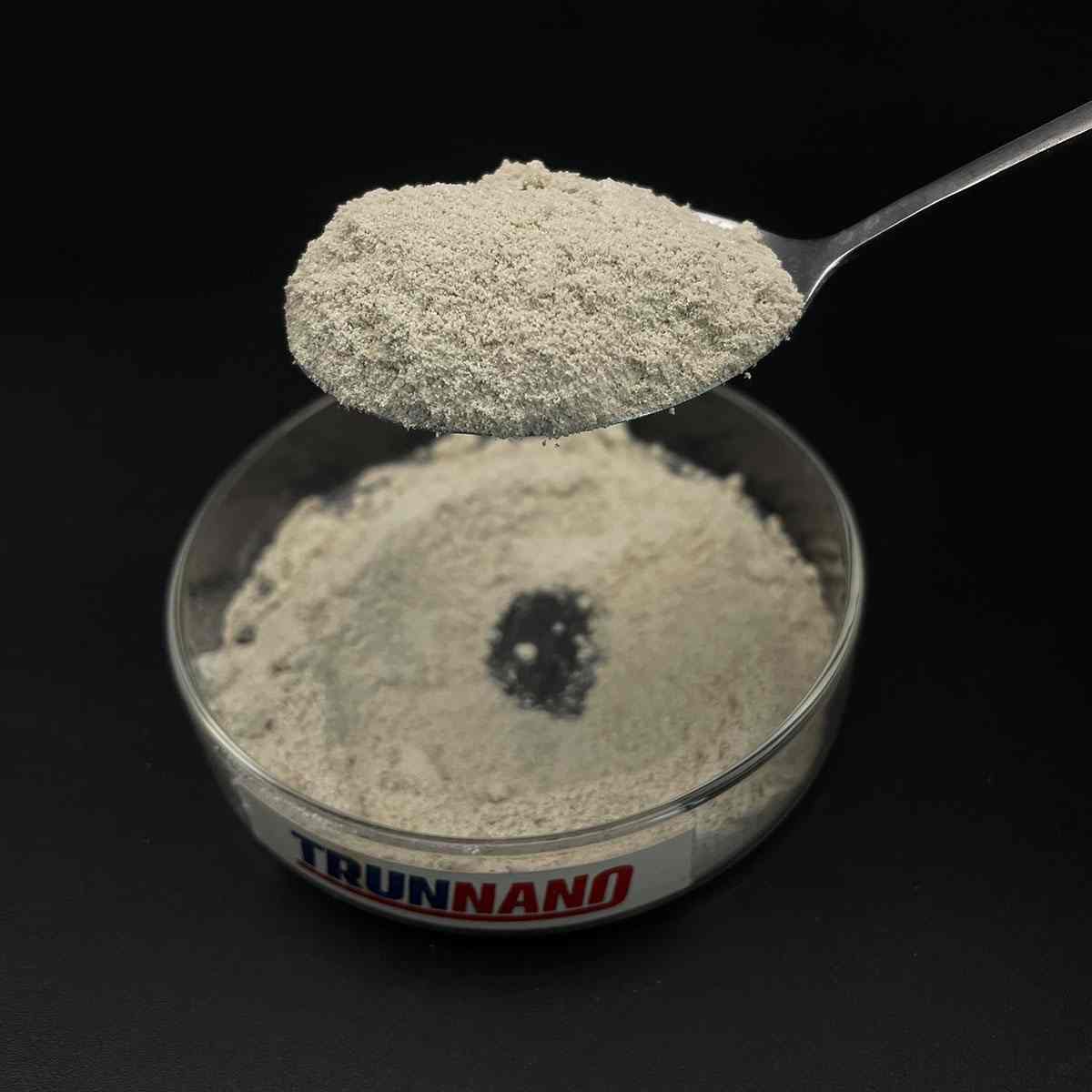
(CdSe PVD Materials High Purity MBE Grade 6N (99.9999%) Sputter Target Cadmium Selenide(CdSe) Powder)
Parameters of CdSe PVD Materials High Purity MBE Grade 6N (99.9999%) Sputter Target Cadmium Selenide(CdSe) Powder
Cadmium Selenide (CdSe), a binary compound of Cadmium and Selenium, is a semiconductor material with exceptional optical and electronic properties, making it a popular choice in various applications, particularly in optoelectronics, photovoltaics, and quantum dot devices. When fabricated using high purity MBE (Molecular Beam Epitaxy) grade materials like 6N (99.9999% purity), CdSe exhibits superior performance and reliability.
CdSe PVD (Physical Vapor Deposition) targets are the starting point for depositing this material onto substrates in thin film processes. The purity level of 6N ensures minimal impurities, which is crucial for maintaining the desired bandgap and minimizing defects that could degrade device performance. The MBE process is a highly controlled method where individual atoms or molecules are precisely manipulated to create epitaxial layers, resulting in films with atomically smooth surfaces and excellent crystal quality.
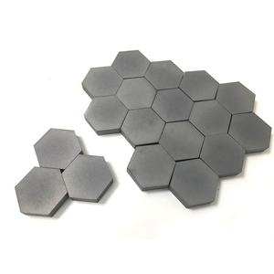
The sputter target for CdSe, typically made from a high-purity ceramic or metal alloy, is carefully prepared to withstand the high temperatures and vacuum conditions during deposition. It is designed to release CdSe particles when bombarded with energetic ions, creating a uniform layer on the substrate. The purity of the target directly affects the film’s purity, as any contaminants introduced during the sputtering process can be detrimental to the final product.
CdSe powders used in MBE often have a submicron particle size, which aids in achieving better film homogeneity and improved optical properties. The powder’s morphology, typically spherical or near-spherical, ensures efficient sintering during the growth process. Additionally, the high purity level reduces the likelihood of grain boundaries, which can act as recombination centers for charge carriers and negatively impact device efficiency.
In photovoltaic devices, CdSe is often combined with other materials like CdTe or CZTS to form multi-junction solar cells, capitalizing on its absorption in the visible spectrum and low cost compared to silicon-based technologies. Quantum dots, made from CdSe, are used in lighting, displays, and biomedical applications due to their tunable bandgap and strong light-emitting capabilities.
Furthermore, CdSe has found applications in photodetectors, sensors, and even as a component in quantum computing due to its potential for spintronics and valleytronics. The high purity of MBE-grown CdSe allows for the exploration of these advanced functionalities with minimal degradation from impurities.
In conclusion, CdSe PVD materials with a 6N purity level, specifically those prepared for MBE, play a vital role in the fabrication of high-quality, optoelectronic devices. Their exceptional purity ensures optimal device performance, while the sputter target enables precise and consistent deposition. As research continues to advance, the importance of high purity materials like CdSe will only grow in the quest for next-generation technologies.

(CdSe PVD Materials High Purity MBE Grade 6N (99.9999%) Sputter Target Cadmium Selenide(CdSe) Powder)
FAQ of Semiconductor Materials
Inquiry us

